Processors
The first Pentium until the current state
Pentium ("Classic")
*Bus width 64 bits
*System bus speed 60 or 66 MHz
*Address bus 32 bits
*Addressable Memory 4 GB
*Virtual Memory 64 TB
*Superscalar architecture brought 5X the performance of the 33 MHz 486DX processor
*Runs on 5 volts
*Used in desktops
*16 KB of L1 cache
*P5 - 0.8 μm process technology
o Introduced March 22, 1993
o Number of transistors 3.1 million
o Socket 4 273 pin PGA processor package
o Package dimensions 2.16" x 2.16"
o Family 5 model 1
o Variants
- 60 MHz with 100 MIPS (70.4 SPECint92, 55.1 SPECfp92 on Xpress 256 KB L2)
- 66 MHz with 112 MIPS (77.9 SPECint92, 63.6 SPECfp92 on Xpress 256 KB L2)
* P54 - 0.6 μm process technology
o Socket 7 296/321 pin PGA package
o Number of transistors 3.2 million
o Variants
- 75 MHz Introduced October 10, 1994
- 90 MHz Introduced March 7, 1994
- 100 MHz Introduced March 7, 1994
- 120 MHz Introduced March 27, 1995
* P54C - 0.35 μm process technology
o Number of transistors 3.3 million
o 90 mm2 die size
o Family 5 model 2
o Variants
- 120 MHz Introduced March, 1995
- 133 MHz Introduced June, 1995
- 150 MHz Introduced January 4, 1996
- 166 MHz Introduced January 4, 1996
- 200 MHz Introduced June 10, 1996
Pentium Pro
*Introduced November 1, 1995
*Precursor to Pentium II and III
*Primarily used in server systems
*Socket 8 processor package (387 pins) (Dual SPGA)
*Number of transistors 5.5 million
*Family 6 model 1
*0.6 μm process technology
o 16 KB L1 cache
o 256 KB integrated L2 cache
o 60 MHz system bus speed
o Variants
-150 MHz
*0.35 μm process technology, or 0.35 μm CPU with 0.6 μm L2 cache
o Number of transistors 5.5 million
o 512 KB or 256 KB integrated L2 cache
o 60 or 66 MHz system bus speed
o Variants
- 166 MHz (66 MHz bus speed, 512 KB 0.35 μm cache) Introduced November 1, 1995
- 180 MHz (60 MHz bus speed, 256 KB 0.6 μm cache) Introduced November 1, 1995
- 200 MHz (66 MHz bus speed, 256 KB 0.6 μm cache) Introduced November 1, 1995
- 200 MHz (66 MHz bus speed, 512 KB 0.35 μm cache) Introduced November 1, 1995
- 200 MHz (66 MHz bus speed, 1 MB 0.35 μm cache) Introduced August 18, 1997
Pentium with MMX Technology
*P55C - 0.35 μm process technology
o Introduced January 8, 1997
o Intel MMX instructions
o Socket 7 296/321 pin PGA (pin grid array) package
o 32 KB L1 cache
o Number of transistors 4.5 million
o System bus speed 66 MHz
o Basic P55C is family 5 model 4, mobile are family 5 model 7 and 8
o Variants
- 166 MHz Introduced January 8, 1997
- 200 MHz Introduced January 8, 1997
- 233 MHz Introduced June 2, 1997
- 166 MHz (Mobile) Introduced January 12, 1998
- 200 MHz (Mobile) Introduced September 8, 1997
- 233 MHz (Mobile) Introduced September 8, 1997
- 266 MHz (Mobile) Introduced January 12, 1998
- 300 MHz (Mobile) Introduced January 7, 1999
Pentium II
* Introduced May 7, 1997
* Pentium Pro with MMX and improved 16-bit performance
* 242-pin Slot 1 (SEC) processor package
* Slot 1
* Number of transistors 7.5 million
* 32 KB L1 cache
* 512 KB - speed external L2 cache
* The only Pentium II that did not have the L2 cache at - speed of the core was the Pentium II 450 PE.
* Klamath - 0.35 μm process technology (233, 266, 300 MHz)
o 66 MHz system bus speed
o Family 6 model 3
o Variants
- 233 MHz Introduced May 7, 1997
- 266 MHz Introduced May 7, 1997
- 300 MHz Introduced May 7, 1997
* Deschutes - 0.25 μm process technology (333, 350, 400, 450 MHz)
o Introduced January 26, 1998
o 66 MHz system bus speed (333 MHz variant), 100 MHz system bus speed for all models after
o Family 6 model 5
o Variants
- 333 MHz Introduced January 26, 1998
- 350 MHz Introduced April 15, 1998
- 400 MHz Introduced April 15, 1998
- 450 MHz Introduced August 24, 1998
- 233 MHz (Mobile) Introduced April 2, 1998
- 266 MHz (Mobile) Introduced April 2, 1998
- 333 MHz Pentium II Overdrive processor for Socket 8 Introduced August 10, 1998; Engineering Sample Photo
- 300 MHz (Mobile) Introduced September 9, 1998
- 333 MHz (Mobile)
Celeron (Pentium II-based)
* Covington - 0.25 μm process technology
o Introduced April 15, 1998
o 242-pin Slot 1 SEPP (Single Edge Processor Package)
o Number of transistors 7.5 million
o 66 MHz system bus speed
o Slot 1
o 32 KB L1 cache
o No L2 cache
o Variants
- 266 MHz Introduced April 15, 1998
- 300 MHz Introduced June 9, 1998
* Mendocino - 0.25 μm process technology
o Introduced August 24, 1998
o 242-pin Slot 1 SEPP (Single Edge Processor Package), Socket 370 PPGA package
o Number of transistors 19 million
o 66 MHz system bus speed
o Slot 1, Socket 370
o 32 KB L1 cache
o 128 KB integrated cache
o Family 6 model 6
o Variants
- 300 A MHz Introduced August 24, 1998
- 333 MHz Introduced August 24, 1998
- 366 MHz Introduced January 4, 1999
- 400 MHz Introduced January 4, 1999
- 433 MHz Introduced March 22, 1999
- 466 MHz
- 500 MHz Introduced August 2, 1999
- 533 MHz Introduced January 4, 2000
- 266 MHz (Mobile)
- 300 MHz (Mobile)
- 333 MHz (Mobile) Introduced April 5, 1999
- 366 MHz (Mobile)
- 400 MHz (Mobile)
- 433 MHz (Mobile)
- 450 MHz (Mobile) Introduced February 14, 2000
- 466 MHz (Mobile)
- 500 MHz (Mobile) Introduced February 14, 2000
Pentium III
* Katmai - 0.25 μm process technology
o Introduced February 26, 1999
o Improved PII, i.e. P6-based core, now including Streaming SIMD Extensions (SSE)
o Number of transistors 9.5 million
o 512 KB ? speed L2 External cache
o 242-pin Slot 1 SECC2 (Single Edge Contact cartridge 2) processor package
o System Bus Speed 100 MHz, 133 MHz (B-models)
o Slot 1
o Family 6 model 7
o Variants
- 450 MHz Introduced February 26, 1999
- 500 MHz Introduced February 26, 1999
- 550 MHz Introduced May 17, 1999
- 600 MHz Introduced August 2, 1999
- 533 MHz Introduced (133 MHz bus speed) September 27, 1999
- 600 MHz Introduced (133 MHz bus speed) September 27, 1999
* Coppermine - 0.18 μm process technology
o Introduced October 25, 1999
o Number of transistors 28.1 million
o 256 KB Advanced Transfer L2 Cache (Integrated)
o 242-pin Slot-1 SECC2 (Single Edge Contact cartridge 2) processor package, 370-pin FC-PGA (Flip-chip pin grid array) package
o System Bus Speed 100 MHz (E-models), 133 MHz (EB models)
o Slot 1, Socket 370
o Family 6 model 8
o Variants
- 500 MHz (100 MHz bus speed)
- 533 MHz
- 550 MHz (100 MHz bus speed)
- 600 MHz
- 600 MHz (100 MHz bus speed)
- 650 MHz (100 MHz bus speed) Introduced October 25, 1999
- 667 MHz Introduced October 25, 1999
- 700 MHz (100 MHz bus speed) Introduced October 25, 1999
- 733 MHz Introduced October 25, 1999
- 750 MHz (100 MHz bus speed) Introduced December 20, 1999
- 800 MHz (100 MHz bus speed) Introduced December 20, 1999
- 850 MHz (100 MHz bus speed) Introduced March 20, 2000
- 866 MHz Introduced March 20, 2000
- 933 MHz Introduced May 24, 2000
- 1000 MHz Introduced March 8, 2000 (Not widely available at time of release)
- 1100 MHz
- 1133 MHz (first version recalled, later re-released)
- 400 MHz (Mobile) Introduced October 25, 1999
- 450 MHz (Mobile) Introduced October 25, 1999
- 500 MHz (Mobile) Introduced October 25, 1999
- 600 MHz (Mobile) Introduced January 18, 2000
- 650 MHz (Mobile) Introduced January 18, 2000
- 700 MHz (Mobile) Introduced April 24, 2000
- 750 MHz (Mobile) Introduced June 19, 2000
- 800 MHz (Mobile) Introduced September 25, 2000
- 850 MHz (Mobile) Introduced September 25, 2000
- 900 MHz (Mobile) Introduced March 19, 2001
- 1000 MHz (Mobile) Introduced March 19, 2001
* Tualatin - 0.13 μm process technology
o Introduced July 2001
o Number of transistors 28.1 million
o 32 KB L1 cache
o 256 KB or 512 KB Advanced Transfer L2 cache (Integrated)
o 370-pin FC-PGA2 (Flip-chip pin grid array) package
o 133 MHz system bus speed
o Socket 370
o Family 6 model 11
o Variants
- 1133 MHz (256 KB L2)
- 1133 MHz (512 KB L2)
- 1200 MHz
- 1266 MHz (512 KB L2)
- 1333 MHz
- 1400 MHz (512 KB L2)
Pentium II and III Xeon
* PII Xeon
o Variants
- 400 MHz Introduced June 29, 1998
- 450 MHz (512 KB L2 Cache) Introduced October 6, 1998
- 450 MHz (1 MB and 2 MB L2 Cache) Introduced January 5, 1999
* PIII Xeon
o Introduced October 25, 1999
o Number of transistors: 9.5 million at 0.25 μm or 28 million at 0.18 μm)
o L2 cache is 256 KB, 1 MB, or 2 MB Advanced Transfer Cache (Integrated)
o Processor Package Style is Single Edge Contact Cartridge (S.E.C.C.2) or SC330
o System Bus Speed 133 MHz (256 KB L2 cache) or 100 MHz (1 - 2 MB L2 cache)
o System Bus Width 64 bit
o Addressable memory 64 GB
o Used in two-way servers and workstations (256 KB L2) or 4- and 8-way servers (1 - 2 MB L2)
o Family 6 model 10
o Variants
- 500 MHz (0.25 μm process) Introduced March 17, 1999
- 550 MHz (0.25 μm process) Introduced August 23, 1999
- 600 MHz (0.18 μm process, 256 KB L2 cache) Introduced October 25, 1999
- 667 MHz (0.18 μm process, 256 KB L2 cache) Introduced October 25, 1999
- 733 MHz (0.18 μm process, 256 KB L2 cache) Introduced October 25, 1999
- 800 MHz (0.18 μm process, 256 KB L2 cache) Introduced January 12, 2000
- 866 MHz (0.18 μm process, 256 KB L2 cache) Introduced April 10, 2000
- 933 MHz (0.18 μm process, 256 KB L2 cache)
- 1000 MHz (0.18 μm process, 256 KB L2 cache) Introduced August 22, 2000
- 700 MHz (0.18 μm process, 1 - 2 MB L2 cache) Introduced May 22, 2000
Celeron (Pentium III Coppermine-based)
* Coppermine-128, 0.18 μm process technology
o Introduced March, 2000
o Streaming SIMD Extensions (SSE)
o Socket 370, FC-PGA processor package
o Number of transistors 28.1 million
o 66 MHz system bus speed, 100 MHz system bus speed from January 3, 2001
o 32 kB L1 cache
o 128 kB Advanced Transfer L2 cache
o Family 6 model 8
o Variants
- 533 MHz
- 566 MHz
- 600 MHz
- 633 MHz Introduced June 26, 2000
- 667 MHz Introduced June 26, 2000
- 700 MHz Introduced June 26, 2000
- 733 MHz Introduced November 13, 2000
- 766 MHz Introduced November 13, 2000
- 800 MHz Introduced January 3, 2001
- 850 MHz Introduced April 9, 2001
- 900 MHz Introduced July 2, 2001
- 950 MHz Introduced August 31, 2001
- 1000 MHz Introduced August 31, 2001
- 1100 MHz Introduced August 31, 2001
- 550 MHz (Mobile)
- 600 MHz (Mobile) Introduced June 19, 2000
- 650 MHz (Mobile) Introduced June 19, 2000
- 700 MHz (Mobile) Introduced September 25, 2000
- 750 MHz (Mobile) Introduced March 19, 2001
- 800 MHz (Mobile)
- 850 MHz (Mobile) Introduced July 2, 2001
- 600 MHz (LV Mobile)
- 500 MHz (ULV Mobile) Introduced January 30, 2001
- 600 MHz (ULV Mobile)
Celeron (Pentium III Tualatin-based)
* Tualatin Celeron - 0.13 μm process technology
o 32 KB L1 cache
o 256 KB Advanced Transfer L2 cache
o 100 MHz system bus speed
o Socket 370
o Family 6 model 11
o Variants
- 1.0 GHz
- 1.1 GHz
- 1.2 GHz
- 1.3 GHz
- 1.4 GHz
Pentium M
* Banias 0.13 μm process technology
o Introduced March 2003
o 64 KB L1 cache
o 1 MB L2 cache (integrated)
o Based on Pentium III core, with SSE2 SIMD instructions and deeper pipeline
o Number of transistors 77 million
o Micro-FCPGA, Micro-FCBGA processor package
o Heart of the Intel mobile "Centrino" system
o 400 MHz Netburst-style system bus
o Family 6 model 9
o Variants
- 900 MHz (Ultra low voltage)
- 1.0 GHz (Ultra low voltage)
- 1.1 GHz (Low voltage)
- 1.2 GHz (Low voltage)
- 1.3 GHz
- 1.4 GHz
- 1.5 GHz
- 1.6 GHz
- 1.7 GHz
* Dothan 0.09 μm (90 nm) process technology
o Introduced May 2004
o 2 MB L2 cache
o Revised data prefetch unit
o 400 MHz Netburst-style system bus
o 21W TDP
o Variants
- 1.00 GHz (Pentium M 723) (Ultra low voltage, 5W TDP)
- 1.10 GHz (Pentium M 733) (Ultra low voltage, 5W TDP)
- 1.20 GHz (Pentium M 753) (Ultra low voltage, 5W TDP)
- 1.30 GHz (Pentium M 718) (Low voltage, 10W TDP)
- 1.40 GHz (Pentium M 738) (Low voltage, 10W TDP)
- 1.50 GHz (Pentium M 758) (Low voltage, 10W TDP)
- 1.60 GHz (Pentium M 778) (Low voltage, 10W TDP)
- 1.40 GHz (Pentium M 710)
- 1.50 GHz (Pentium M 715)
- 1.60 GHz (Pentium M 725)
- 1.70 GHz (Pentium M 735)
- 1.80 GHz (Pentium M 745)
- 2.00 GHz (Pentium M 755)
- 2.10 GHz (Pentium M 765)
* Dothan 533 0.09 μm (90 nm) process technology
o Introduced Q1 2005
o Same as Dothan except with a 533 MHz NetBurst-style system bus and 27W TDP
o Variants
- 1.60 GHz (Pentium M 730)
- 1.73 GHz (Pentium M 740)
- 1.86 GHz (Pentium M 750)
- 2.00 GHz (Pentium M 760)
- 2.13 GHz (Pentium M 770)
- 2.26 GHz (Pentium M 780)
* Stealey 0.09 μm (90 nm) process technology
o Introduced Q2 2007
o 512 KB L2, 3W TDP
o Variants
- 600 MHz (A100)
- 800 MHz (A110)
Celeron M
* Banias-512 0.13 μm process technology
o Introduced March 2003
o 64 KB L1 cache
o 512 KB L2 cache (integrated)
o SSE2 SIMD instructions
o No SpeedStep technology, is not part of the 'Centrino' package
o Family 6 model 9
o Variants
- 310 - 1.20 GHz
- 320 - 1.30 GHz
- 330 - 1.40 GHz
- 340 - 1.50 GHz
* Dothan-1024 90 nm process technology
o 64 KB L1 cache
o 1 MB L2 cache (integrated)
o SSE2 SIMD instructions
o No SpeedStep technology, is not part of the 'Centrino' package
o Variants
- 350 - 1.30 GHz
- 350J - 1.30 GHz, with Execute Disable bit
- 360 - 1.40 GHz
- 360J - 1.40 GHz, with Execute Disable bit
- 370 - 1.50 GHz, with Execute Disable bit
- Family 6, Model 13, Stepping 8[2]
- 380 - 1.60 GHz, with Execute Disable bit
- 390 - 1.70 GHz, with Execute Disable bit
* Yonah-1024 65 nm process technology
o 64 KB L1 cache
o 1 MB L2 cache (integrated)
o SSE3 SIMD instructions, 533 MHz front-side bus, execute-disable bit
o No SpeedStep technology, is not part of the 'Centrino' package
o Variants
- 410 - 1.46 GHz
- 420 - 1.60 GHz,
- 423 - 1.06 GHz (ultra low voltage)
- 430 - 1.73 GHz
- 440 - 1.86 GHz
- 443 - 1.20 GHz (ultra low voltage)
- 450 - 2.00 GHz
Intel Core
* Yonah 0.065 μm (65 nm) process technology
o Introduced January 2006
o 667 MHz frontside bus
o 2 MB (Shared on Duo) L2 cache
o SSE3 SIMD instructions
o 31W TDP (T**** versions)
o Variants:
- Intel Core Duo T2700 2.33 GHz
- Intel Core Duo T2600 2.16 GHz
- Intel Core Duo T2500 2.00 GHz
- Intel Core Duo T2400 1.83 GHz
- Intel Core Duo T2300 1.66 GHz
- Intel Core Duo T2050 1.60 GHz
- Intel Core Duo T2080 1.73 GHz
- Intel Core Duo T2300e 1.66 GHz
- Intel Core Duo T2080 1.73 GHz
- Intel Core Duo L2500 1.83 GHz (Low voltage, 15W TDP)
- Intel Core Duo L2400 1.66 GHz (Low voltage, 15W TDP)
- Intel Core Duo L2300 1.50 GHz (Low voltage, 15W TDP)
- Intel Core Duo U2500 1.20 GHz (Ultra low voltage, 9W TDP)
- Intel Core Solo T1350 1.86 GHz (533 FSB)
- Intel Core Solo T1300 1.66 GHz
- Intel Core Solo T1200 1.50 GHz [3]
Dual-Core Xeon LV
* Sossaman 0.065 μm (65 nm) process technology
o Introduced March 2006
o Based on Yonah core, with SSE3 SIMD instructions
o 667 MHz frontside bus
o 2 MB Shared L2 cache
o Variants
- 2.0 GHz
Intel Pentium Dual-Core
* 0.065 μm (65 nm) process technology
o 533 MHz frontside bus
o 1 MB Shared L2 cache
o SSE3 SIMD instructions
o Variants:
- Pentium dual-core T2080 1.73 GHz
- Pentium dual-core T2060 1.60 GHz
AMD

AMD processors latest model is AMD Phenom X4 9950. This models come out on July 1st 2008.
AMD Phenom X4 9950 models is the best for Energy Efficient, small form, factor PCs and Home Theater PCs. It is pair with AMD 7 series chipset for optimal performance-per-decibel AMD ati Radeon HD graphics for scalable gaming performance at an exceptional price. AMD Phenom X4 9950 also best for the HD gaming with performance tuning.
This AMD model also already fix the TLB erratum problems on the 9900. In this model AMD had using 65nm silicon on Insulator process technology. AMD Phenom X4 9950 has the CPU/FSB multiplier unlocked for easier overclocking. In the others Phenom X4 9000 series processors had a slower 1.6GHZ - 1.8GHz memory controller but Phenom X49950 has a faster memory controller, it is 2.0 GHz !
AMD also said that, this processors had using a Cool ‘n’ Quiet 2.0 Technology. This technique can improve overall power savings and no nosing when you using the computer. That is why this technology call Cool ‘n’ Quiet 2.0 Techonology.
Reference
http://www.amd.com/us-en/Processors/ProductInformation/0,,30_118_15331_15332%5E15333,00.html
Diffrences between AMD and Intel

Reference :
http://www.intel.com/
http://www.amd.com/
Other processor type
Other than Intel & AMD, there are many other processors used in the micro class computers such as Cyrix, NexGen and many more.
One of the other processors is from this VIA Technology. VIA offers a wide range of power efficient processors that are driving system innovation in the PC, client, ultra mobile and embedded markets. Providing industry leading performance per watt, miniaturization, low power consumption and compatibility with a complete range of feature rich VIA digital media chipsets, VIA processors are powering the new generation of embedded, mobile and consumer electronics devices.
VIA processors of at least 800MHz are recognized by Microsoft as a processor option in a Windows Vista Capable PC. One of the most recent version of the VIA processor is the new VIA Nano, from the VIA Technology family. This VIA Nano processor was launched early this year.
The VIA Nano processor are targeted to specific applications based on power consumption and performance criteria, ranging from higher performance for mainstream desktop and notebook PCs, fan less operation to power saving capabilities for battery operated mobile devices.


VIA Nano is the first 64-bit, superscalar processors in VIA's x86 platform portfolio, and have been specifically designed to revitalize traditional desktop and notebook PC markets, delivering truly optimized performance for the most demanding computing, entertainment and connectivity applications.
VIA Nano processor offers as much as four times the performance within the same power range to extend VIA's performance per watt leadership, with an easy upgrade path for current system or board designs.
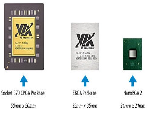
Unlike Intel and AMD, VIA Nano uses two distinct development codenames for each of its CPU cores. Fujitsu acts as the most common manufacturer of this processor. VIA Nano processor comes with ultra compact dimensions, enabling a new generation of small form factor designs and new, smaller applications for the x86 platforms.
~Features of VIA Nano Processor~
64-bit Superscalar Micro Architecture
- Supports a full 64-bit instruction set and provides for macro-fusion and micro-fusion functionality, and sophisticated branch prediction for greater processor efficiency and performance
High-Performance Computation and Media Processing
- The high-speed, low power VIA V4 Front Side Bus (FSB) starting at 800MHz, plus a high floating point unit, support for new instructions, and two 64KB L1 caches and 1MB exclusive L2 cache with 16-way associativity gives a big boost to multimedia performance
Advanced Power and Thermal Management
- Aggressive management of active power includes Adaptive PowerSaver Technology, new circuit techniques and mechanisms for managing the die temperature, reducing power draw and improving thermal management
Greener Technology
- Product will be halogen-free and lead-free at launch, helping to promote a cleaner environment and more sustainable computing
Enhanced VIA PadLock Security Engine
- Industry-leading on-die hardware cryptographic acceleration and security features
~Characteristics of different VIA Nano Models~

~References:~
http://www.via.com.tw/en/products/processors/nano/
http://www.via.com.tw/en/products/processors/
http://www.via.com.tw/en/products/processors/
http://en.wikipedia.org/wiki/VIA_Isaiah
http://www.via.com.tw/en/resources/pressroom/pressrelease.jsp?press_release_no=2369
http://www.via.com.tw/en/downloads/whitepapers/processors/WP080529VIA_Nano.pdf
http://xtreview.com/addcomment-id-5339-view-Via-nano-isaiah.html
Pentium ("Classic")
*Bus width 64 bits
*System bus speed 60 or 66 MHz
*Address bus 32 bits
*Addressable Memory 4 GB
*Virtual Memory 64 TB
*Superscalar architecture brought 5X the performance of the 33 MHz 486DX processor
*Runs on 5 volts
*Used in desktops
*16 KB of L1 cache
*P5 - 0.8 μm process technology
o Introduced March 22, 1993
o Number of transistors 3.1 million
o Socket 4 273 pin PGA processor package
o Package dimensions 2.16" x 2.16"
o Family 5 model 1
o Variants
- 60 MHz with 100 MIPS (70.4 SPECint92, 55.1 SPECfp92 on Xpress 256 KB L2)
- 66 MHz with 112 MIPS (77.9 SPECint92, 63.6 SPECfp92 on Xpress 256 KB L2)
* P54 - 0.6 μm process technology
o Socket 7 296/321 pin PGA package
o Number of transistors 3.2 million
o Variants
- 75 MHz Introduced October 10, 1994
- 90 MHz Introduced March 7, 1994
- 100 MHz Introduced March 7, 1994
- 120 MHz Introduced March 27, 1995
* P54C - 0.35 μm process technology
o Number of transistors 3.3 million
o 90 mm2 die size
o Family 5 model 2
o Variants
- 120 MHz Introduced March, 1995
- 133 MHz Introduced June, 1995
- 150 MHz Introduced January 4, 1996
- 166 MHz Introduced January 4, 1996
- 200 MHz Introduced June 10, 1996
Pentium Pro
*Introduced November 1, 1995
*Precursor to Pentium II and III
*Primarily used in server systems
*Socket 8 processor package (387 pins) (Dual SPGA)
*Number of transistors 5.5 million
*Family 6 model 1
*0.6 μm process technology
o 16 KB L1 cache
o 256 KB integrated L2 cache
o 60 MHz system bus speed
o Variants
-150 MHz
*0.35 μm process technology, or 0.35 μm CPU with 0.6 μm L2 cache
o Number of transistors 5.5 million
o 512 KB or 256 KB integrated L2 cache
o 60 or 66 MHz system bus speed
o Variants
- 166 MHz (66 MHz bus speed, 512 KB 0.35 μm cache) Introduced November 1, 1995
- 180 MHz (60 MHz bus speed, 256 KB 0.6 μm cache) Introduced November 1, 1995
- 200 MHz (66 MHz bus speed, 256 KB 0.6 μm cache) Introduced November 1, 1995
- 200 MHz (66 MHz bus speed, 512 KB 0.35 μm cache) Introduced November 1, 1995
- 200 MHz (66 MHz bus speed, 1 MB 0.35 μm cache) Introduced August 18, 1997
Pentium with MMX Technology
*P55C - 0.35 μm process technology
o Introduced January 8, 1997
o Intel MMX instructions
o Socket 7 296/321 pin PGA (pin grid array) package
o 32 KB L1 cache
o Number of transistors 4.5 million
o System bus speed 66 MHz
o Basic P55C is family 5 model 4, mobile are family 5 model 7 and 8
o Variants
- 166 MHz Introduced January 8, 1997
- 200 MHz Introduced January 8, 1997
- 233 MHz Introduced June 2, 1997
- 166 MHz (Mobile) Introduced January 12, 1998
- 200 MHz (Mobile) Introduced September 8, 1997
- 233 MHz (Mobile) Introduced September 8, 1997
- 266 MHz (Mobile) Introduced January 12, 1998
- 300 MHz (Mobile) Introduced January 7, 1999
Pentium II
* Introduced May 7, 1997
* Pentium Pro with MMX and improved 16-bit performance
* 242-pin Slot 1 (SEC) processor package
* Slot 1
* Number of transistors 7.5 million
* 32 KB L1 cache
* 512 KB - speed external L2 cache
* The only Pentium II that did not have the L2 cache at - speed of the core was the Pentium II 450 PE.
* Klamath - 0.35 μm process technology (233, 266, 300 MHz)
o 66 MHz system bus speed
o Family 6 model 3
o Variants
- 233 MHz Introduced May 7, 1997
- 266 MHz Introduced May 7, 1997
- 300 MHz Introduced May 7, 1997
* Deschutes - 0.25 μm process technology (333, 350, 400, 450 MHz)
o Introduced January 26, 1998
o 66 MHz system bus speed (333 MHz variant), 100 MHz system bus speed for all models after
o Family 6 model 5
o Variants
- 333 MHz Introduced January 26, 1998
- 350 MHz Introduced April 15, 1998
- 400 MHz Introduced April 15, 1998
- 450 MHz Introduced August 24, 1998
- 233 MHz (Mobile) Introduced April 2, 1998
- 266 MHz (Mobile) Introduced April 2, 1998
- 333 MHz Pentium II Overdrive processor for Socket 8 Introduced August 10, 1998; Engineering Sample Photo
- 300 MHz (Mobile) Introduced September 9, 1998
- 333 MHz (Mobile)
Celeron (Pentium II-based)
* Covington - 0.25 μm process technology
o Introduced April 15, 1998
o 242-pin Slot 1 SEPP (Single Edge Processor Package)
o Number of transistors 7.5 million
o 66 MHz system bus speed
o Slot 1
o 32 KB L1 cache
o No L2 cache
o Variants
- 266 MHz Introduced April 15, 1998
- 300 MHz Introduced June 9, 1998
* Mendocino - 0.25 μm process technology
o Introduced August 24, 1998
o 242-pin Slot 1 SEPP (Single Edge Processor Package), Socket 370 PPGA package
o Number of transistors 19 million
o 66 MHz system bus speed
o Slot 1, Socket 370
o 32 KB L1 cache
o 128 KB integrated cache
o Family 6 model 6
o Variants
- 300 A MHz Introduced August 24, 1998
- 333 MHz Introduced August 24, 1998
- 366 MHz Introduced January 4, 1999
- 400 MHz Introduced January 4, 1999
- 433 MHz Introduced March 22, 1999
- 466 MHz
- 500 MHz Introduced August 2, 1999
- 533 MHz Introduced January 4, 2000
- 266 MHz (Mobile)
- 300 MHz (Mobile)
- 333 MHz (Mobile) Introduced April 5, 1999
- 366 MHz (Mobile)
- 400 MHz (Mobile)
- 433 MHz (Mobile)
- 450 MHz (Mobile) Introduced February 14, 2000
- 466 MHz (Mobile)
- 500 MHz (Mobile) Introduced February 14, 2000
Pentium III
* Katmai - 0.25 μm process technology
o Introduced February 26, 1999
o Improved PII, i.e. P6-based core, now including Streaming SIMD Extensions (SSE)
o Number of transistors 9.5 million
o 512 KB ? speed L2 External cache
o 242-pin Slot 1 SECC2 (Single Edge Contact cartridge 2) processor package
o System Bus Speed 100 MHz, 133 MHz (B-models)
o Slot 1
o Family 6 model 7
o Variants
- 450 MHz Introduced February 26, 1999
- 500 MHz Introduced February 26, 1999
- 550 MHz Introduced May 17, 1999
- 600 MHz Introduced August 2, 1999
- 533 MHz Introduced (133 MHz bus speed) September 27, 1999
- 600 MHz Introduced (133 MHz bus speed) September 27, 1999
* Coppermine - 0.18 μm process technology
o Introduced October 25, 1999
o Number of transistors 28.1 million
o 256 KB Advanced Transfer L2 Cache (Integrated)
o 242-pin Slot-1 SECC2 (Single Edge Contact cartridge 2) processor package, 370-pin FC-PGA (Flip-chip pin grid array) package
o System Bus Speed 100 MHz (E-models), 133 MHz (EB models)
o Slot 1, Socket 370
o Family 6 model 8
o Variants
- 500 MHz (100 MHz bus speed)
- 533 MHz
- 550 MHz (100 MHz bus speed)
- 600 MHz
- 600 MHz (100 MHz bus speed)
- 650 MHz (100 MHz bus speed) Introduced October 25, 1999
- 667 MHz Introduced October 25, 1999
- 700 MHz (100 MHz bus speed) Introduced October 25, 1999
- 733 MHz Introduced October 25, 1999
- 750 MHz (100 MHz bus speed) Introduced December 20, 1999
- 800 MHz (100 MHz bus speed) Introduced December 20, 1999
- 850 MHz (100 MHz bus speed) Introduced March 20, 2000
- 866 MHz Introduced March 20, 2000
- 933 MHz Introduced May 24, 2000
- 1000 MHz Introduced March 8, 2000 (Not widely available at time of release)
- 1100 MHz
- 1133 MHz (first version recalled, later re-released)
- 400 MHz (Mobile) Introduced October 25, 1999
- 450 MHz (Mobile) Introduced October 25, 1999
- 500 MHz (Mobile) Introduced October 25, 1999
- 600 MHz (Mobile) Introduced January 18, 2000
- 650 MHz (Mobile) Introduced January 18, 2000
- 700 MHz (Mobile) Introduced April 24, 2000
- 750 MHz (Mobile) Introduced June 19, 2000
- 800 MHz (Mobile) Introduced September 25, 2000
- 850 MHz (Mobile) Introduced September 25, 2000
- 900 MHz (Mobile) Introduced March 19, 2001
- 1000 MHz (Mobile) Introduced March 19, 2001
* Tualatin - 0.13 μm process technology
o Introduced July 2001
o Number of transistors 28.1 million
o 32 KB L1 cache
o 256 KB or 512 KB Advanced Transfer L2 cache (Integrated)
o 370-pin FC-PGA2 (Flip-chip pin grid array) package
o 133 MHz system bus speed
o Socket 370
o Family 6 model 11
o Variants
- 1133 MHz (256 KB L2)
- 1133 MHz (512 KB L2)
- 1200 MHz
- 1266 MHz (512 KB L2)
- 1333 MHz
- 1400 MHz (512 KB L2)
Pentium II and III Xeon
* PII Xeon
o Variants
- 400 MHz Introduced June 29, 1998
- 450 MHz (512 KB L2 Cache) Introduced October 6, 1998
- 450 MHz (1 MB and 2 MB L2 Cache) Introduced January 5, 1999
* PIII Xeon
o Introduced October 25, 1999
o Number of transistors: 9.5 million at 0.25 μm or 28 million at 0.18 μm)
o L2 cache is 256 KB, 1 MB, or 2 MB Advanced Transfer Cache (Integrated)
o Processor Package Style is Single Edge Contact Cartridge (S.E.C.C.2) or SC330
o System Bus Speed 133 MHz (256 KB L2 cache) or 100 MHz (1 - 2 MB L2 cache)
o System Bus Width 64 bit
o Addressable memory 64 GB
o Used in two-way servers and workstations (256 KB L2) or 4- and 8-way servers (1 - 2 MB L2)
o Family 6 model 10
o Variants
- 500 MHz (0.25 μm process) Introduced March 17, 1999
- 550 MHz (0.25 μm process) Introduced August 23, 1999
- 600 MHz (0.18 μm process, 256 KB L2 cache) Introduced October 25, 1999
- 667 MHz (0.18 μm process, 256 KB L2 cache) Introduced October 25, 1999
- 733 MHz (0.18 μm process, 256 KB L2 cache) Introduced October 25, 1999
- 800 MHz (0.18 μm process, 256 KB L2 cache) Introduced January 12, 2000
- 866 MHz (0.18 μm process, 256 KB L2 cache) Introduced April 10, 2000
- 933 MHz (0.18 μm process, 256 KB L2 cache)
- 1000 MHz (0.18 μm process, 256 KB L2 cache) Introduced August 22, 2000
- 700 MHz (0.18 μm process, 1 - 2 MB L2 cache) Introduced May 22, 2000
Celeron (Pentium III Coppermine-based)
* Coppermine-128, 0.18 μm process technology
o Introduced March, 2000
o Streaming SIMD Extensions (SSE)
o Socket 370, FC-PGA processor package
o Number of transistors 28.1 million
o 66 MHz system bus speed, 100 MHz system bus speed from January 3, 2001
o 32 kB L1 cache
o 128 kB Advanced Transfer L2 cache
o Family 6 model 8
o Variants
- 533 MHz
- 566 MHz
- 600 MHz
- 633 MHz Introduced June 26, 2000
- 667 MHz Introduced June 26, 2000
- 700 MHz Introduced June 26, 2000
- 733 MHz Introduced November 13, 2000
- 766 MHz Introduced November 13, 2000
- 800 MHz Introduced January 3, 2001
- 850 MHz Introduced April 9, 2001
- 900 MHz Introduced July 2, 2001
- 950 MHz Introduced August 31, 2001
- 1000 MHz Introduced August 31, 2001
- 1100 MHz Introduced August 31, 2001
- 550 MHz (Mobile)
- 600 MHz (Mobile) Introduced June 19, 2000
- 650 MHz (Mobile) Introduced June 19, 2000
- 700 MHz (Mobile) Introduced September 25, 2000
- 750 MHz (Mobile) Introduced March 19, 2001
- 800 MHz (Mobile)
- 850 MHz (Mobile) Introduced July 2, 2001
- 600 MHz (LV Mobile)
- 500 MHz (ULV Mobile) Introduced January 30, 2001
- 600 MHz (ULV Mobile)
Celeron (Pentium III Tualatin-based)
* Tualatin Celeron - 0.13 μm process technology
o 32 KB L1 cache
o 256 KB Advanced Transfer L2 cache
o 100 MHz system bus speed
o Socket 370
o Family 6 model 11
o Variants
- 1.0 GHz
- 1.1 GHz
- 1.2 GHz
- 1.3 GHz
- 1.4 GHz
Pentium M
* Banias 0.13 μm process technology
o Introduced March 2003
o 64 KB L1 cache
o 1 MB L2 cache (integrated)
o Based on Pentium III core, with SSE2 SIMD instructions and deeper pipeline
o Number of transistors 77 million
o Micro-FCPGA, Micro-FCBGA processor package
o Heart of the Intel mobile "Centrino" system
o 400 MHz Netburst-style system bus
o Family 6 model 9
o Variants
- 900 MHz (Ultra low voltage)
- 1.0 GHz (Ultra low voltage)
- 1.1 GHz (Low voltage)
- 1.2 GHz (Low voltage)
- 1.3 GHz
- 1.4 GHz
- 1.5 GHz
- 1.6 GHz
- 1.7 GHz
* Dothan 0.09 μm (90 nm) process technology
o Introduced May 2004
o 2 MB L2 cache
o Revised data prefetch unit
o 400 MHz Netburst-style system bus
o 21W TDP
o Variants
- 1.00 GHz (Pentium M 723) (Ultra low voltage, 5W TDP)
- 1.10 GHz (Pentium M 733) (Ultra low voltage, 5W TDP)
- 1.20 GHz (Pentium M 753) (Ultra low voltage, 5W TDP)
- 1.30 GHz (Pentium M 718) (Low voltage, 10W TDP)
- 1.40 GHz (Pentium M 738) (Low voltage, 10W TDP)
- 1.50 GHz (Pentium M 758) (Low voltage, 10W TDP)
- 1.60 GHz (Pentium M 778) (Low voltage, 10W TDP)
- 1.40 GHz (Pentium M 710)
- 1.50 GHz (Pentium M 715)
- 1.60 GHz (Pentium M 725)
- 1.70 GHz (Pentium M 735)
- 1.80 GHz (Pentium M 745)
- 2.00 GHz (Pentium M 755)
- 2.10 GHz (Pentium M 765)
* Dothan 533 0.09 μm (90 nm) process technology
o Introduced Q1 2005
o Same as Dothan except with a 533 MHz NetBurst-style system bus and 27W TDP
o Variants
- 1.60 GHz (Pentium M 730)
- 1.73 GHz (Pentium M 740)
- 1.86 GHz (Pentium M 750)
- 2.00 GHz (Pentium M 760)
- 2.13 GHz (Pentium M 770)
- 2.26 GHz (Pentium M 780)
* Stealey 0.09 μm (90 nm) process technology
o Introduced Q2 2007
o 512 KB L2, 3W TDP
o Variants
- 600 MHz (A100)
- 800 MHz (A110)
Celeron M
* Banias-512 0.13 μm process technology
o Introduced March 2003
o 64 KB L1 cache
o 512 KB L2 cache (integrated)
o SSE2 SIMD instructions
o No SpeedStep technology, is not part of the 'Centrino' package
o Family 6 model 9
o Variants
- 310 - 1.20 GHz
- 320 - 1.30 GHz
- 330 - 1.40 GHz
- 340 - 1.50 GHz
* Dothan-1024 90 nm process technology
o 64 KB L1 cache
o 1 MB L2 cache (integrated)
o SSE2 SIMD instructions
o No SpeedStep technology, is not part of the 'Centrino' package
o Variants
- 350 - 1.30 GHz
- 350J - 1.30 GHz, with Execute Disable bit
- 360 - 1.40 GHz
- 360J - 1.40 GHz, with Execute Disable bit
- 370 - 1.50 GHz, with Execute Disable bit
- Family 6, Model 13, Stepping 8[2]
- 380 - 1.60 GHz, with Execute Disable bit
- 390 - 1.70 GHz, with Execute Disable bit
* Yonah-1024 65 nm process technology
o 64 KB L1 cache
o 1 MB L2 cache (integrated)
o SSE3 SIMD instructions, 533 MHz front-side bus, execute-disable bit
o No SpeedStep technology, is not part of the 'Centrino' package
o Variants
- 410 - 1.46 GHz
- 420 - 1.60 GHz,
- 423 - 1.06 GHz (ultra low voltage)
- 430 - 1.73 GHz
- 440 - 1.86 GHz
- 443 - 1.20 GHz (ultra low voltage)
- 450 - 2.00 GHz
Intel Core
* Yonah 0.065 μm (65 nm) process technology
o Introduced January 2006
o 667 MHz frontside bus
o 2 MB (Shared on Duo) L2 cache
o SSE3 SIMD instructions
o 31W TDP (T**** versions)
o Variants:
- Intel Core Duo T2700 2.33 GHz
- Intel Core Duo T2600 2.16 GHz
- Intel Core Duo T2500 2.00 GHz
- Intel Core Duo T2400 1.83 GHz
- Intel Core Duo T2300 1.66 GHz
- Intel Core Duo T2050 1.60 GHz
- Intel Core Duo T2080 1.73 GHz
- Intel Core Duo T2300e 1.66 GHz
- Intel Core Duo T2080 1.73 GHz
- Intel Core Duo L2500 1.83 GHz (Low voltage, 15W TDP)
- Intel Core Duo L2400 1.66 GHz (Low voltage, 15W TDP)
- Intel Core Duo L2300 1.50 GHz (Low voltage, 15W TDP)
- Intel Core Duo U2500 1.20 GHz (Ultra low voltage, 9W TDP)
- Intel Core Solo T1350 1.86 GHz (533 FSB)
- Intel Core Solo T1300 1.66 GHz
- Intel Core Solo T1200 1.50 GHz [3]
Dual-Core Xeon LV
* Sossaman 0.065 μm (65 nm) process technology
o Introduced March 2006
o Based on Yonah core, with SSE3 SIMD instructions
o 667 MHz frontside bus
o 2 MB Shared L2 cache
o Variants
- 2.0 GHz
Intel Pentium Dual-Core
* 0.065 μm (65 nm) process technology
o 533 MHz frontside bus
o 1 MB Shared L2 cache
o SSE3 SIMD instructions
o Variants:
- Pentium dual-core T2080 1.73 GHz
- Pentium dual-core T2060 1.60 GHz
AMD

AMD processors latest model is AMD Phenom X4 9950. This models come out on July 1st 2008.
AMD Phenom X4 9950 models is the best for Energy Efficient, small form, factor PCs and Home Theater PCs. It is pair with AMD 7 series chipset for optimal performance-per-decibel AMD ati Radeon HD graphics for scalable gaming performance at an exceptional price. AMD Phenom X4 9950 also best for the HD gaming with performance tuning.
This AMD model also already fix the TLB erratum problems on the 9900. In this model AMD had using 65nm silicon on Insulator process technology. AMD Phenom X4 9950 has the CPU/FSB multiplier unlocked for easier overclocking. In the others Phenom X4 9000 series processors had a slower 1.6GHZ - 1.8GHz memory controller but Phenom X49950 has a faster memory controller, it is 2.0 GHz !
AMD also said that, this processors had using a Cool ‘n’ Quiet 2.0 Technology. This technique can improve overall power savings and no nosing when you using the computer. That is why this technology call Cool ‘n’ Quiet 2.0 Techonology.
Reference
http://www.amd.com/us-en/Processors/ProductInformation/0,,30_118_15331_15332%5E15333,00.html
Diffrences between AMD and Intel

Reference :
http://www.intel.com/
http://www.amd.com/
Other processor type
Other than Intel & AMD, there are many other processors used in the micro class computers such as Cyrix, NexGen and many more.
One of the other processors is from this VIA Technology. VIA offers a wide range of power efficient processors that are driving system innovation in the PC, client, ultra mobile and embedded markets. Providing industry leading performance per watt, miniaturization, low power consumption and compatibility with a complete range of feature rich VIA digital media chipsets, VIA processors are powering the new generation of embedded, mobile and consumer electronics devices.
VIA processors of at least 800MHz are recognized by Microsoft as a processor option in a Windows Vista Capable PC. One of the most recent version of the VIA processor is the new VIA Nano, from the VIA Technology family. This VIA Nano processor was launched early this year.
The VIA Nano processor are targeted to specific applications based on power consumption and performance criteria, ranging from higher performance for mainstream desktop and notebook PCs, fan less operation to power saving capabilities for battery operated mobile devices.

VIA Nano is the first 64-bit, superscalar processors in VIA's x86 platform portfolio, and have been specifically designed to revitalize traditional desktop and notebook PC markets, delivering truly optimized performance for the most demanding computing, entertainment and connectivity applications.
VIA Nano processor offers as much as four times the performance within the same power range to extend VIA's performance per watt leadership, with an easy upgrade path for current system or board designs.
Unlike Intel and AMD, VIA Nano uses two distinct development codenames for each of its CPU cores. Fujitsu acts as the most common manufacturer of this processor. VIA Nano processor comes with ultra compact dimensions, enabling a new generation of small form factor designs and new, smaller applications for the x86 platforms.
~Features of VIA Nano Processor~
64-bit Superscalar Micro Architecture
- Supports a full 64-bit instruction set and provides for macro-fusion and micro-fusion functionality, and sophisticated branch prediction for greater processor efficiency and performance
High-Performance Computation and Media Processing
- The high-speed, low power VIA V4 Front Side Bus (FSB) starting at 800MHz, plus a high floating point unit, support for new instructions, and two 64KB L1 caches and 1MB exclusive L2 cache with 16-way associativity gives a big boost to multimedia performance
Advanced Power and Thermal Management
- Aggressive management of active power includes Adaptive PowerSaver Technology, new circuit techniques and mechanisms for managing the die temperature, reducing power draw and improving thermal management
Greener Technology
- Product will be halogen-free and lead-free at launch, helping to promote a cleaner environment and more sustainable computing
Enhanced VIA PadLock Security Engine
- Industry-leading on-die hardware cryptographic acceleration and security features
~Characteristics of different VIA Nano Models~

~References:~
http://www.via.com.tw/en/products/processors/nano/
http://www.via.com.tw/en/products/processors/
http://www.via.com.tw/en/products/processors/
http://en.wikipedia.org/wiki/VIA_Isaiah
http://www.via.com.tw/en/resources/pressroom/pressrelease.jsp?press_release_no=2369
http://www.via.com.tw/en/downloads/whitepapers/processors/WP080529VIA_Nano.pdf
http://xtreview.com/addcomment-id-5339-view-Via-nano-isaiah.html
Comments